EECS 143 Microfabrication Technology
1. Introduction
The purpose of the 4-point probe is to measure the resistivity of any semiconductor material. It can measure either bulk or thin film specimen, each of which consists of a different expression. The derivation will be shown in this tutorial.
The 4-point probe setup used in the EECS 143 instructional lab consists of four equally spaced tungsten metal tips with finite radius. Each tip is supported by springs on the other end to minimize sample damage during probing. The four metal tips are part of an auto-mechanical stage which travels up and down during measurements. A high impedance current source is used to supply current through the outer two probes; a voltmeter measures the voltage across the inner two probes (See Figure 1) to determine the sample resistivity. Typical probe spacing s ~ 1 mm.
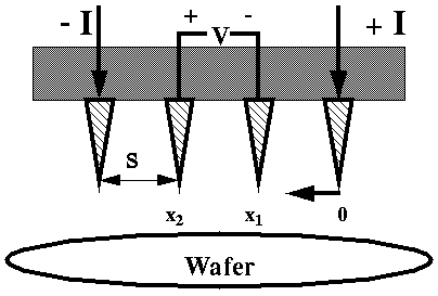
Figure 1. Schematic of 4-point probe configuration
2. Theory
- Bulk SampleIn our derivations for this section, we assume that the metal tip is infinitesimal and samples are semi-infinite in lateral dimension. For bulk samples where the sample thickness t >> s, the probe spacing, we assume a spherical protrusion of current emanating from the outer probe tips. The differential resistance is:

We carry out the integration between the inner probe tips (where the voltage is measured):
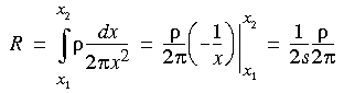
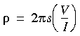
where probe spacing is uniformly s. Due to the superposition of current at the outer two tips, R = V/2I. Thus, we arrive at the expression for bulk resistivity:
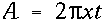
- Thin SheetFor a very thin layer (thickness t << s), we get current rings instead of spheres. Therefore, the expression for the area
 . The derivation is as follows:
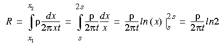
Consequently, for R = V/2I, the sheet resistivity for a thin sheet is:
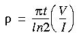
Note that this expression is independent of the probe spacing s. Furthermore, this latter expression is frequently used for characterization semiconductor layers, such as a diffused N+ region in a p-type substrate. In general, the sheet resistivity
 can be expressed as:
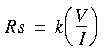
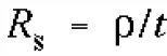
where the factor k is a geometric factor. In the case of a semi-infinite thin sheet, k = 4.53, which is just
 from the derivation. The factor k will be different for non-ideal samples.
3. Operation Procedures
The following steps should be taken in the following sequence:
- Turn on the voltmeter, set the mode to DC and voltage range to 200 mV.
- Place wafer onto the probe stage.
- Flip the toggle switch located atop the probe station from “NEUTRAL” TO “DOWN”.
- Watch the probe casing lower until the probes stabilize on the wafer.
- Return the toggle switch of the probe station to the “NEUTRAL” position.
- Turn on the current source by turning the black switch “S1” to the “ON” position.
- Set the current to the desired level, and proceed with measuring the voltage across the inner two probes. Map the wafer.
- When measurement is finished, shut off the current source by turning the switch “S1” to the “OFF” position.
- Flip the probe station toggle switch from “NEUTRAL” to “UP”.
- Wait until the probe casing is all the way up, then set the toggle switch back to “NEUTRAL”.
- Turn off voltmeter.
James Chan, Spring 1994
The original page can be found here: http://www-inst.eecs.berkeley.edu/~ee143/fa10/lab/four_point_probe.pdf
Four-Point-Probes is a division of Bridge Technology. To request further information please call Bridge Technology at (480) 219-9007 or send e-mail to Joshua Bridge at: sales@bridgetec.com